Convert Circuit Diagram To Pcb Layout Online
How to convert pcb to schematic diagram? How to convert schemetic diagram into pcb layout step 2 of circuit Printed circuit board design, diagram and assembly
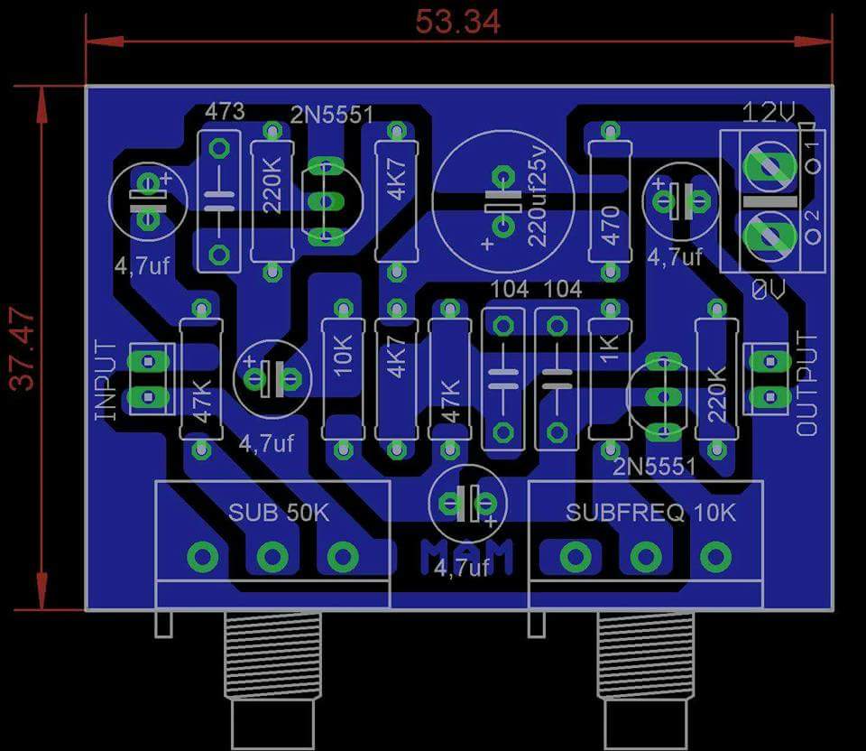
Schematic of circuit diagram and Actual PCB layout of the system
How to convert pcb to schematic diagram? Smps fullbridge pfc schematic + pcb layout pdf Pcb guideline altium
How to convert schematic diagram into pcb layout in easyeda online pcb
Simple 555 timer ‘door bell’ is great for learning autodesk circuitsProteus convert simulation Pcb schematic diagram layout easyeda convert intoBaru pcb subwoofer, skema pcb.
Subwoofer circuit amplifier skema frequency elcircuit adjust rangkaian ziyaret speaker elektronik letak tata disimpanPcb layout circuit schematic layer rules multi basic software pcbs using board electronic do standard printed pads protel proteus auto Pcb layoutPcb circuits timer adafruit autodesk door importance learning schematic pcbs breadboard.

Pcb schematic make convert layout symbol custom circuit project basics associated automatically footprints editor each will
Convert circuit to pcbDiagram schematic basics circuits lying mastering component How to convert pcb to schematic diagram?How to design a pcb layout.
Signal transmissionSmps pcb pfc layout 4kva schematic fullbridge pdf circuit electronic ni tested Pcb schematic komatsu startsCircuitos impresos pcbs circuito impreso.
Schematics according restore raypcb convert protel orcad
Make sure to consider these factors when creating a pcb layoutConvert schemetic circuit Schematic convertHow to convert pcb to schematic diagram?.
How to design a pcb layoutMastering the art of pcb design basics Schematic of circuit diagram and actual pcb layout of the systemConvert simulation circuit into pcb ready circuit in proteus by auto.

Schematic diagram
13 basic rules of pcb layoutReverse engineering high speed pcb board layout diagram .
.


Reverse Engineering High Speed PCB Board Layout Diagram

SMPS FULLBRIDGE PFC Schematic + PCB Layout PDF - Electronic Circuit

convert circuit to PCB - NI Community

How to Convert PCB to Schematic Diagram? - RAYPCB

Convert simulation circuit into PCB ready circuit in Proteus by Auto

How to Convert schematic diagram into PCB layout in Easyeda Online PCB

How to Design a PCB Layout - Circuit Basics

How to Convert PCB to Schematic Diagram? - RAYPCB